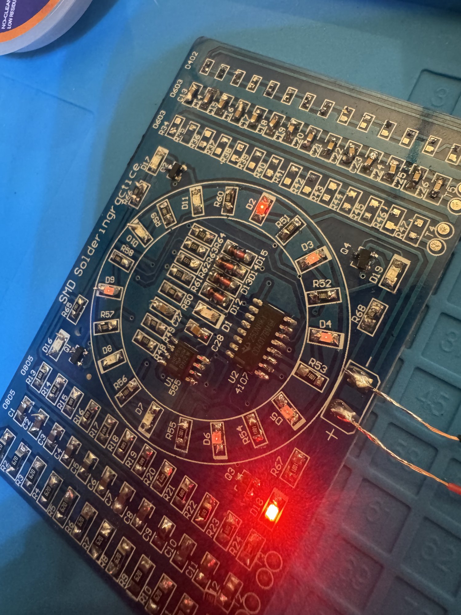
I had been looking at the lamp side of the board and thinking the 1K resistors for the ring were missing from the kit, until I realized I had already used them. The 1001 parts I put in the 0603 practice column are noticeably bigger than those pads. They are 0805s, and they were meant for the ring. The smaller 1R5 parts were the ones that belonged in the practice column. That also cleared up a confusion I had been carrying around about the markings: the 1206, 0805, 0603, and 0402 labels on the board are package sizes, and the numbers printed on the parts themselves, 1001, 103, 106, 1R5, are the values. I had been mixing those up more than I care to admit. Putting 0805s on 0603 pads may also have had something to do with the confusing continuity readings I was getting on that column, though I am not sure.
Getting them off the column
So I desoldered all fourteen of the 1001s, to use them plus one unused spare on the ring. Most of the pads stayed intact, but the one at R35 lifted while I was taking the part off. I left it alone rather than making it worse.
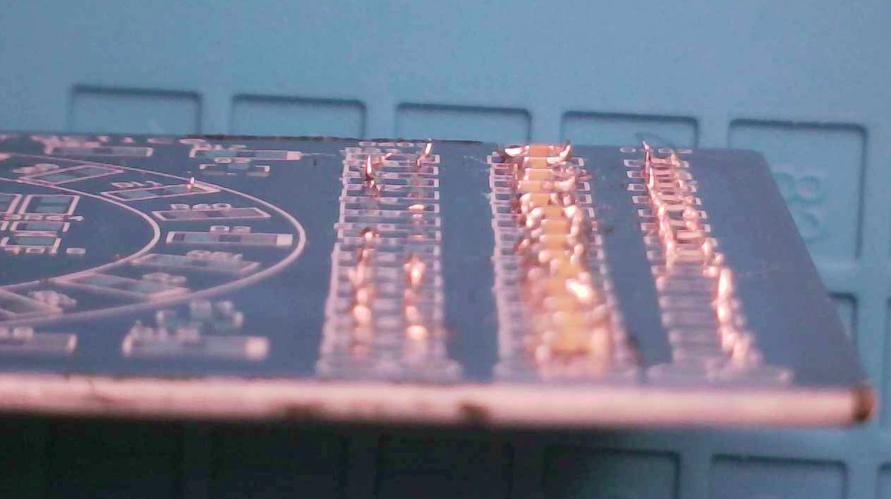
I did two passes over the empty pads with flux, copper wick, and alcohol. The first one took down the worst of the leftover solder, and the second got more of it, though some still remains. I decided that was far enough. I had learned something about cleaning pads after a removal, and I wanted to get on with the lamp circuit.
The lamp ring
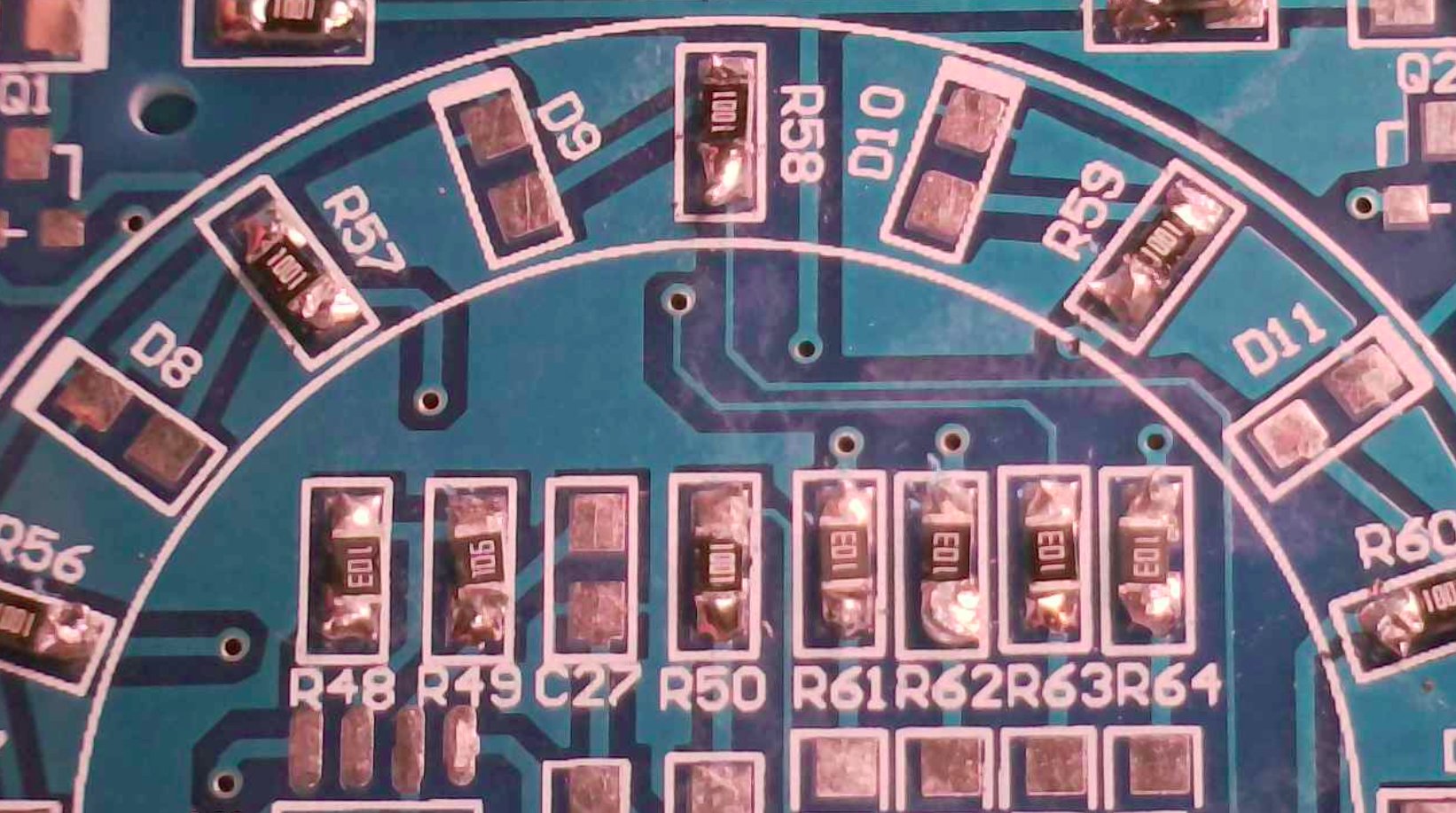
I put the fifteen 1001s around the ring, along with the 103s at R48 and R61 through R64, the 106 at R49, and the capacitors at C27 and C28. I am starting to feel the joints getting more consistent, and I am moving faster between steps than I was a few sessions ago. I also cleaned some excess solder off the ring resistors, though I did not photograph that step. All fifteen of the 1001s checked out on the meter.
The first SMT chip
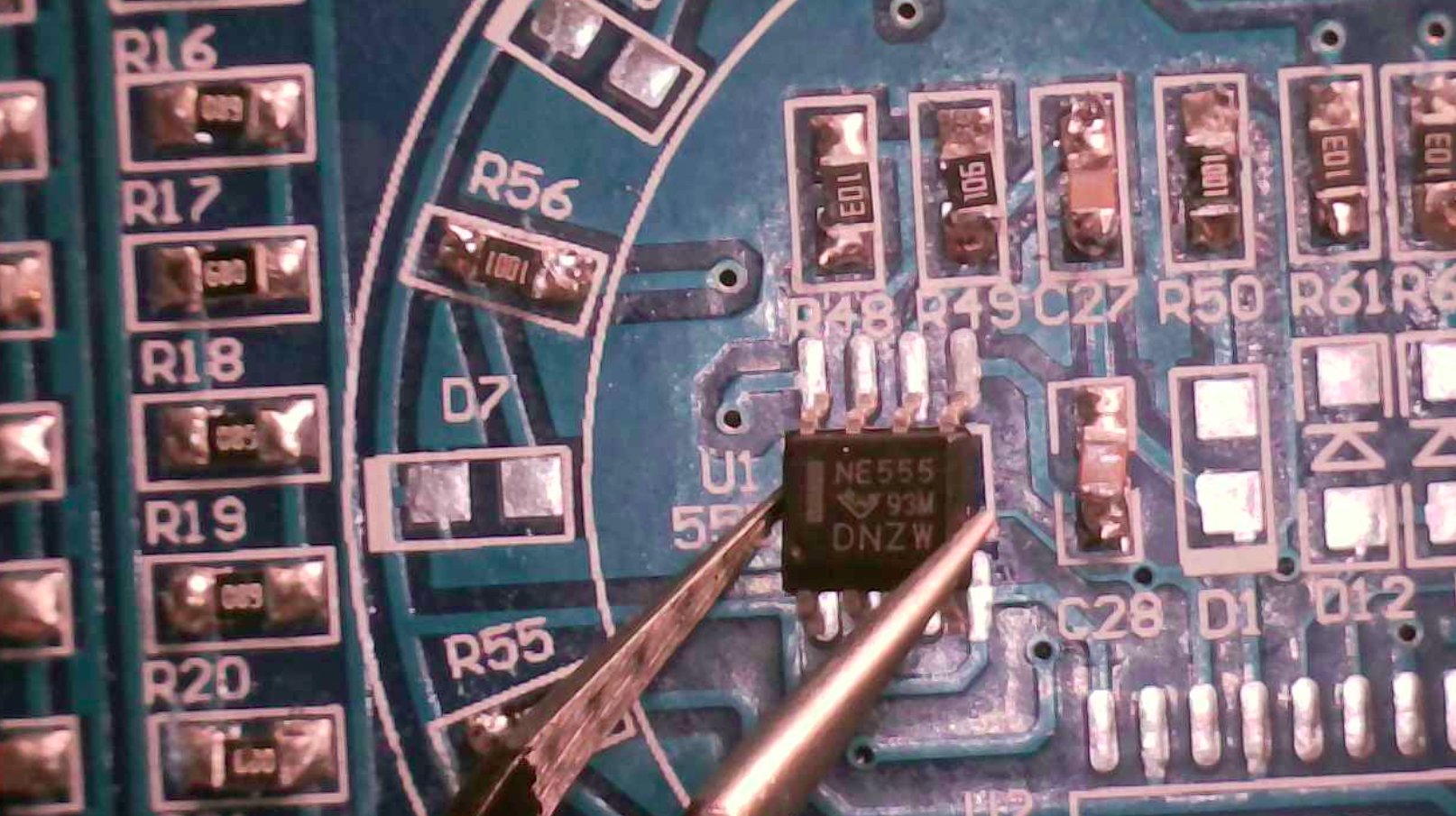
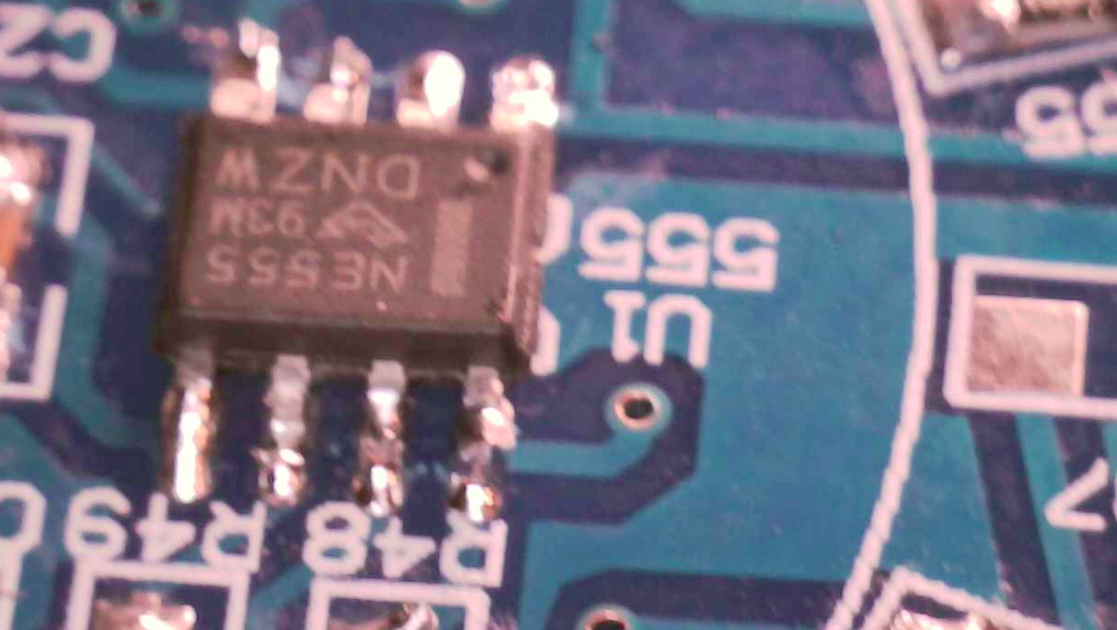
Then I placed my first SMT chip, the NE555 at U1. I lined the dot up with the notch on the silkscreen, held it with the tweezers under the microscope, tacked one corner, and then soldered the rest of the pins. All eight came out clean, with no bridges that I could see.
Sixteen tighter pins
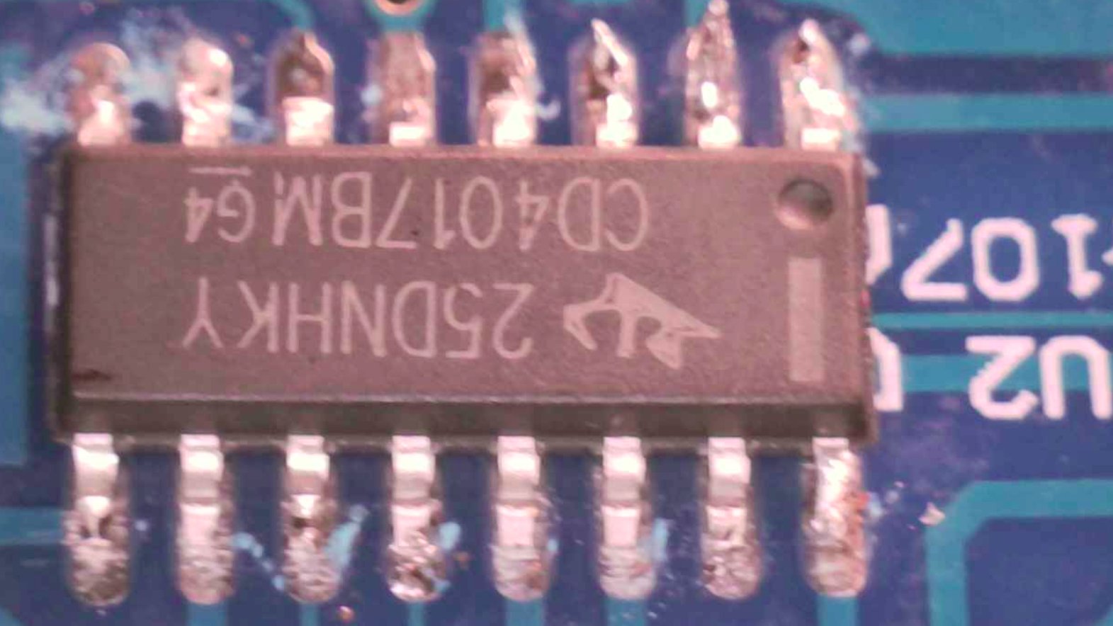
The CD4017 at U2 has sixteen pins, and they sit closer together than the 555's. I tacked one corner, checked the alignment, and worked my way around. I am learning to respect what "less solder" means with this pin spacing.
The transistors
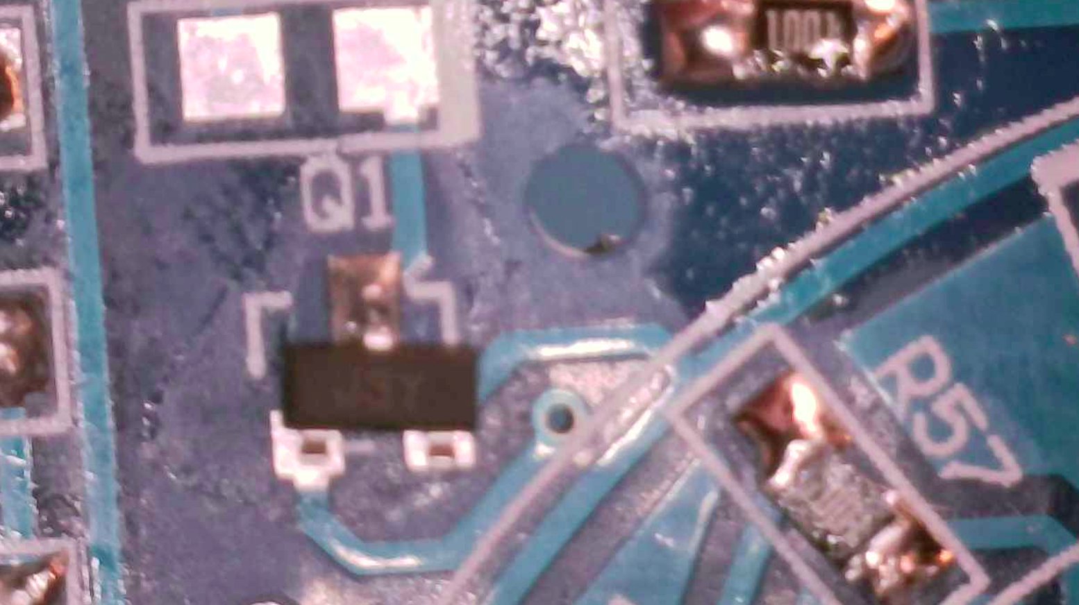
Q1 through Q4 are SOT-23 transistors, and those were definitely a bit tricky, with two legs on one side and a single leg on the other. I tacked the single leg first and then did the others. In diode mode, all four of them read the same 0.845 volts, which was a relief.
The glass diodes
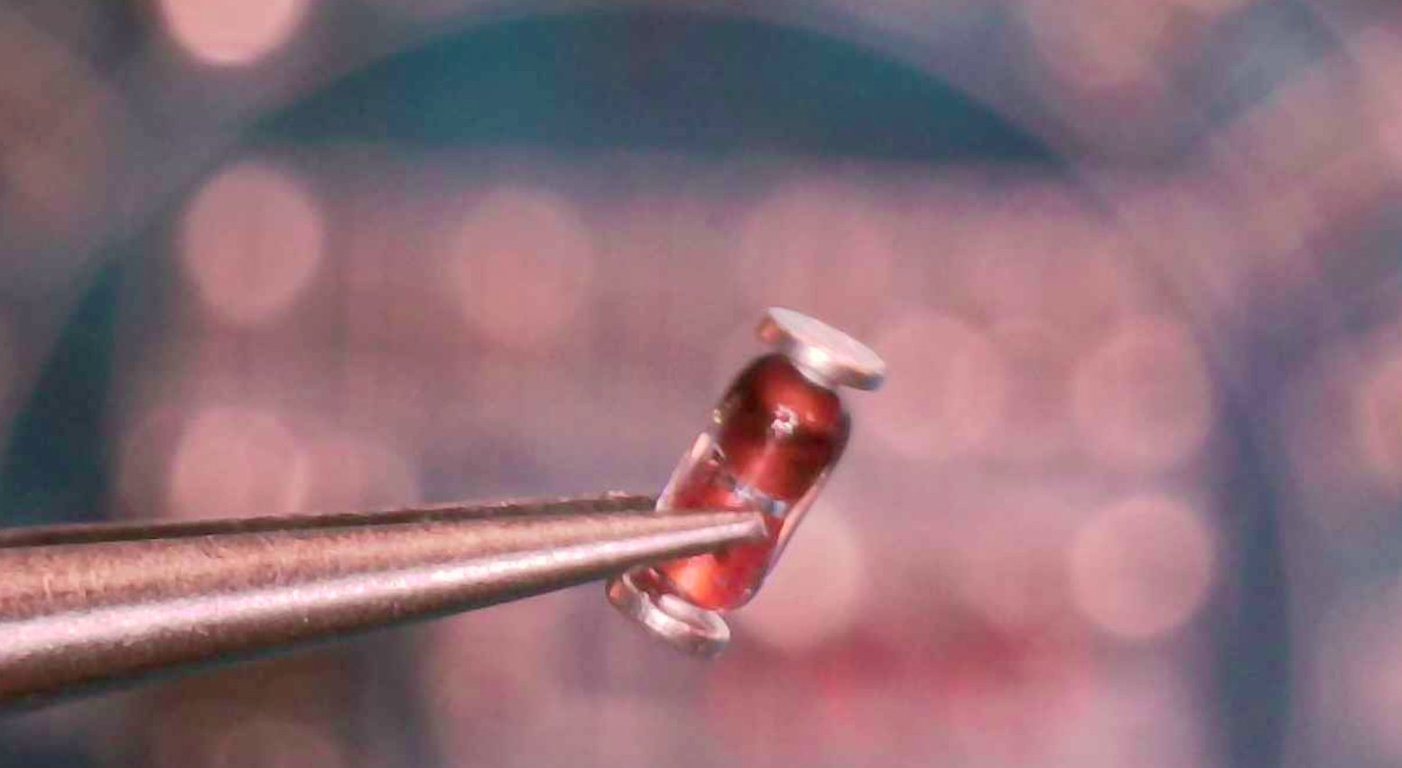
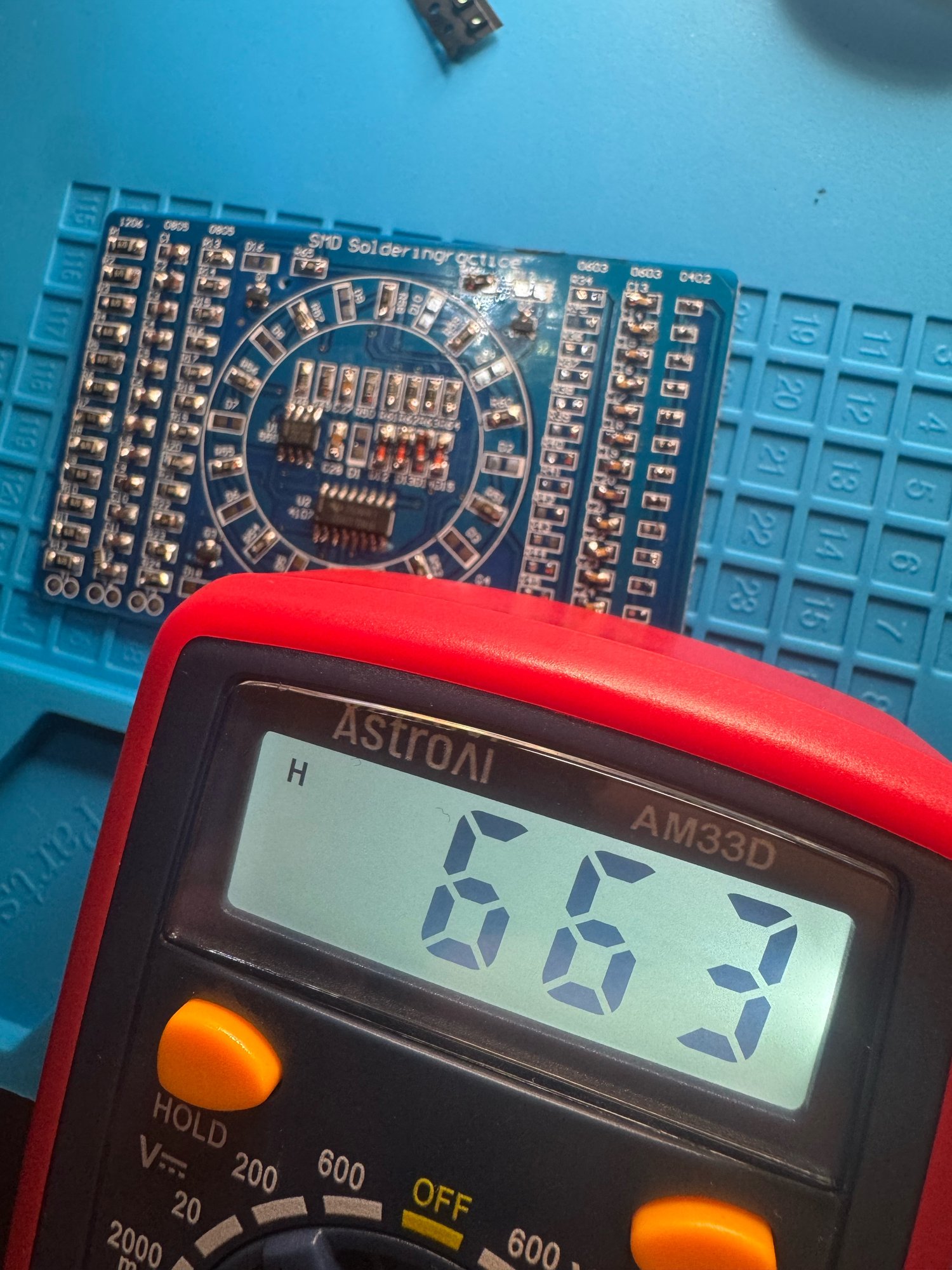
The LL34 diodes at D12 through D15 were a different kind of puzzle. They are little glass capsules, and the cathode band is almost invisible on these, at least to my eyes, even under the microscope. I gave up trying to squint at it and used the meter, which told me the orientation clearly enough. Once they were on the board, all four read about 0.66 volts. The one I photographed was 663 millivolts. To take that picture I had to keep the probes on the part and press the meter's HOLD button with my nose, which worked, and which I will probably be doing again.
The LEDs, and a cable for power
The LEDs have clear lenses, so you can't tell the color until they light up. I tested each one in diode mode before I placed it, and I matched the cathode to the mark on the board. The kit was supposed to include eleven red LEDs for the ring and four blue ones for the corners, but there were no blue ones in the bag at all, which I am chalking up to sloppy packing on an inexpensive kit. I used what I had, so the corner LEDs are red as well.
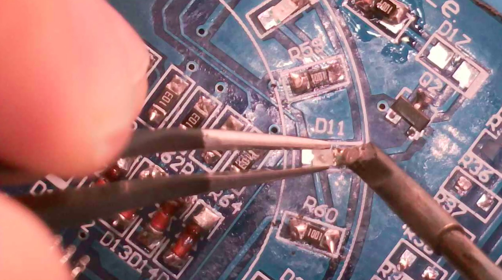
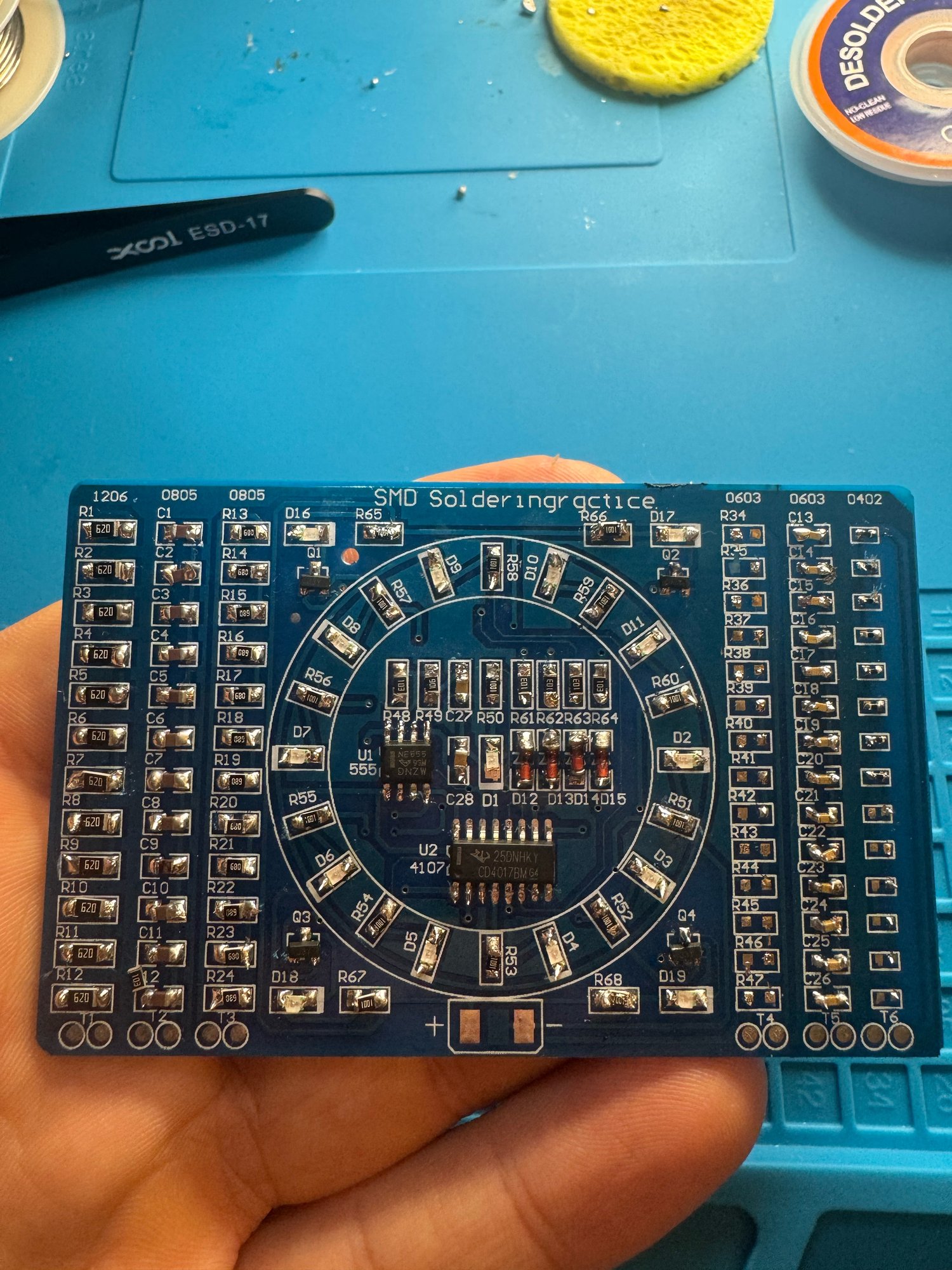
With the LEDs on, every part of the lamp circuit was in place, except for the + and − pads at the bottom of the board.
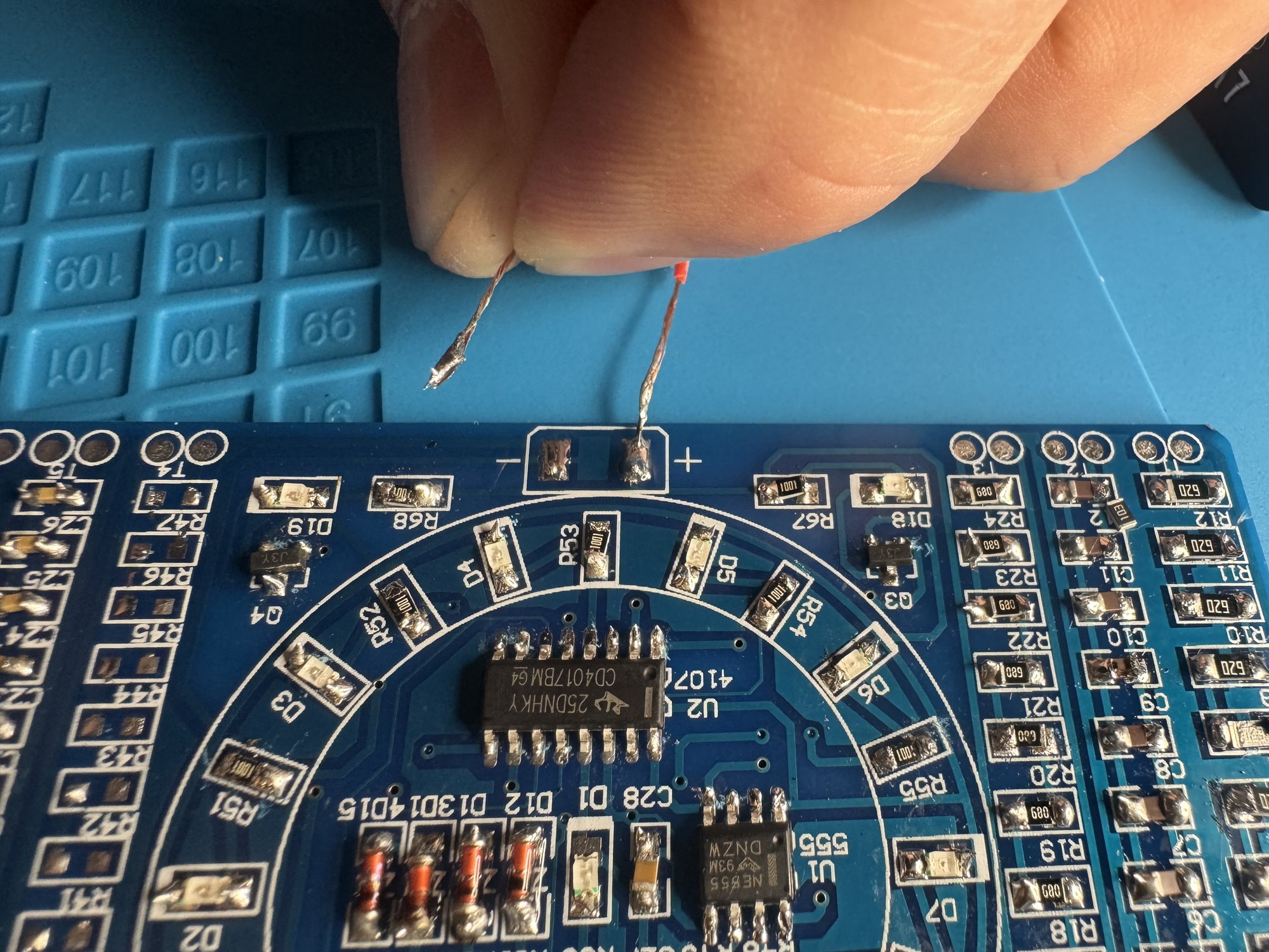
The kit did not come with a power source, so I cut the micro end off a spare USB cable I was happy to sacrifice. Inside it were the usual red, black, green, and white wires. Red is the 5 volt line and black is ground, and the green and white are data lines I did not need, so I trimmed those back. I twisted and tinned the red and black, tinned the two pads, and soldered the red wire to +.
That is when the cordless iron died, one joint from the finish. I had to put it on the charger for a few minutes before I could solder the black wire to −.
First light
I plugged the cable in, and the ring lit up, or part of it did. At first I thought only D18 and D2 were flashing, but more of them are blinking too. They are just faint, and hard to see under the bench light. D18, one of the corner LEDs, is clearly the brightest, and since the kit had no blue LEDs, that one being red is what I expected. I was plugged into a USB hub at first, and I also tried a wall charger, which did not change what I was seeing, so I don't think this is a power problem.
I do not know yet why the ring is not showing a single chasing red dot, with only one LED lit at a time. Several of them glow faintly instead. I am stopping here for the night. A whole board is soldered and powered, and it is doing something, even if the chase is not right yet. I am feeling accomplished. In the morning I will look more carefully at the 4017 and at the dimmer LEDs.